
Contents
- Why HBM Creates a Difficult Thermal Path
- Total Power vs. Local Heat Flux
- Where Hotspots Form in an HBM Stack
- What an HBM Hotspot Actually Costs
- Why HBM4 Raises the Thermal Challenge
- Managing HBM Hotspots Across the Thermal Path
- Why TIM Selection Decides the Outcome
- FAQs
- References
As AI accelerators push toward higher compute density and memory bandwidth, High Bandwidth Memory (HBM) has become essential to advanced semiconductor packaging. But stacking multiple memory dies beside a high-power GPU or accelerator creates a difficult thermal problem: heat generation is highly localized, while the path available to remove it is increasingly constrained.
HBM hotspot management is therefore not simply about lowering the average package temperature. The more major challenge is controlling peak temperature and heat gradients at localized thermal hotspots. Three metrics govern that work: maximum junction temperature (Tmax), local gradients (ΔT within the stack), and local power density (W/cm²). Designing against these, rather than package averages, reveals the vulnerable regions.
Why HBM Creates a Difficult Thermal Path
HBM stacks DRAM dies vertically, connected through through-silicon vias (TSVs), then sits alongside a GPU on an interposer, typically in a CoWoS-class 2.5D architecture. This improves electrical performance and density at a thermal cost: heat must cross multiple silicon dies, bonding layers, interconnects, and package interfaces before reaching the cooling system.
Total Power vs. Local Heat Flux
Total package power determines how much heat the cooling system must reject. Local heat flux determines how hard a hotspot is to cool. Two packages with similar total power behave very differently if one concentrates more heat into a smaller area. That matters in heterogeneous AI packages, where logic and HBM occupy different footprints and generate non-uniform thermal loads. Effective management accounts for both total load and local W/cm².
Where Hotspots Form in an HBM Stack
HBM does not heat uniformly. Conditions vary by layer and region, depending on memory activity, stack architecture, and the surrounding package.
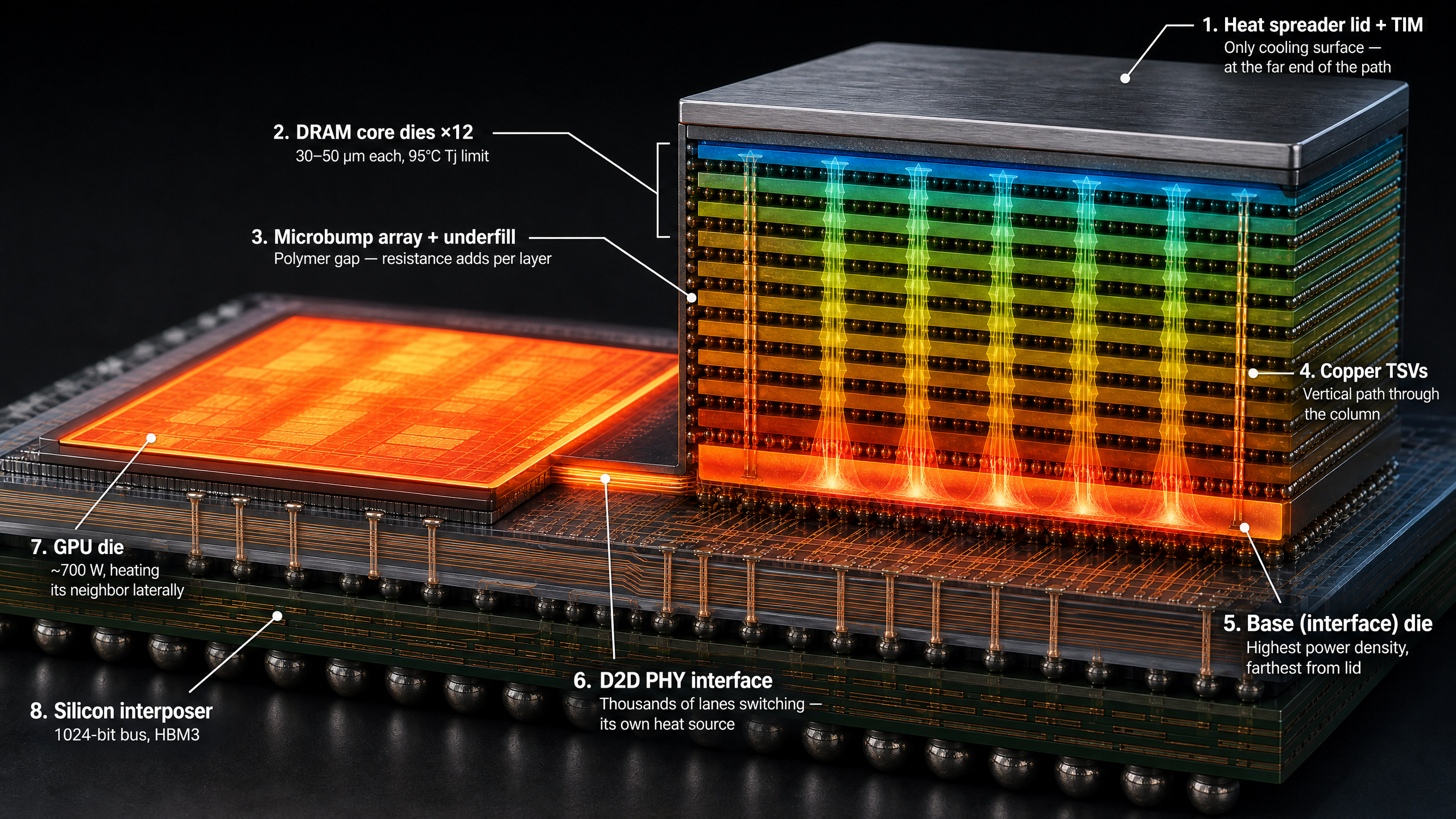
The Logic/Base Die as a Critical Thermal Region
The base or logic die combines active circuitry with the longest thermal path to the cooling interface. In a 12-high HBM3 stack, it must push heat through the entire column of DRAM dies above it before reaching a spreader or lid. Each inter-die gap is bridged by microbump arrays filled with underfill polymer, a poor thermal conductor, so inter-die resistance adds up with every layer of stack height. Patent analysis of a 2024 Huawei Technologies disclosure reports that in a four-layer HBM2 stack, the difference between hottest and coolest points on the bottom die alone can reach 24°C. Micron documents a related case: when the logic die’s high-power peripheral region extends beyond the DRAM footprint, routing that heat through the full stack can raise Tmax by roughly 30°C.
Neighboring Processor Heat Changes the Picture
HBM cannot be analyzed independently from the accelerator beside it. A high-power logic die injects heat laterally through the package structure, so a memory stack can run hotter than its neighbors while having less headroom: DRAM-process dies are typically specified to 95°C junction temperature, below the 105°C commonly permitted for peripheral CMOS logic. HBM thermal design therefore requires package-level co-optimization, not isolated component analysis. SK hynix’s “iHBM” architecture embeds cooling elements into the die-to-die (D2D) physical layer, reporting roughly a 30% reduction in interface thermal resistance.
What an HBM Hotspot Actually Costs
Missing the temperature target on HBM rarely announces itself as a failure. It shows up as lost throughput.
- Refresh overhead climbs, and the loop reinforces itself. Retention time falls as temperature rises, so hotter dies need more frequent refresh. Above roughly 85°C, parts commonly move to a doubled refresh rate. Those cycles consume bandwidth compute never sees, so the workload runs longer and the die runs hotter still.
- Throttling follows. Past safe limits, requests to heated regions are blocked, or clocks are pulled back to protect the hardware, and performance drops with them.
- Error rates rise. Intel’s per-channel thermal management disclosure notes that the risk of unrecoverable memory errors climbs with temperature, causing crashes and downtime. That matters far more in a training run measured in weeks than a benchmark measured in seconds.
- Mechanical damage accumulates. Copper expands at 17.5×10⁻⁶/K and silicon at roughly 2.6×10⁻⁶/K. (Thermal Expansion Coefficient of Metals & Materials, 2026) Cycling across that mismatch drives warpage, solder joint fatigue, TIM pump-out, and delamination.
Why HBM4 Raises the Thermal Challenge
JEDEC published the HBM4 standard (JESD270-4) in April 2025. It doubles the interface to 2048 bits, doubles independent channels per stack from 16 to 32 with two pseudo-channels each, and pushes bandwidth toward 2 TB/s per stack. Stacks run 4-high to 16-high on 24 Gb or 32 Gb dies, reaching 64 GB, and the base logic die moves onto advanced foundry logic processes. All three major suppliers reached volume shipment during 2026.
Each change improves bandwidth and complicates thermal design. Taller stacks mean longer vertical heat paths; wider interfaces mean more switching energy at the D2D layer; more capacity means more heat in the same footprint, next to processors that are also getting hotter.
Managing HBM Hotspots Across the Thermal Path
No single material or cooling technology fixes every bottleneck. Treat the thermal path as one integrated system.
Die- and Stack-Level Thermal Design
TSV architecture, thermally conductive structures, die placement, bonding interfaces, and underfill all shape how heat moves through the stack. As height and power density increase, internal thermal resistance becomes the dominant lever on peak temperatures and gradients.
Package-Level Heat Transfer
Thermal interface materials (TIMs), heat spreaders, lid structures, and bond-line thickness all shape the path from stack to cooling interface. The objective is not maximum conductivity but minimum interface resistance, while handling warpage, surface variation, and height differences.
Metal Interfaces: Where Polymers Run Out
Polymer TIMs reach a conductivity ceiling. Metal interfaces push it higher, at the cost of process complexity.
Indium solder TIMs reflow into an intermetallic bond, the lowest interfacial resistance of any TIM class, with no pump-out and little sensitivity to bond-line variation. The constraint is process: pure indium melts below the board-level reflow peak, so it re-melts during downstream assembly. Amkor found that lower-silver alloys degrade coverage and worsen warpage, with delamination at the die edges, while raising silver reduces conductivity and stiffens the joint.
Liquid metal trades differently. Gallium-based alloys conform without clamping force and tolerate large height variation, but are electrically conductive, corrosive to aluminum and copper, and need engineered barriers. Stability is unsettled: a four-year aging study found Galinstan began solidifying in year two and had fully solidified by year four.
Heat Spreading and Thermomechanical Management
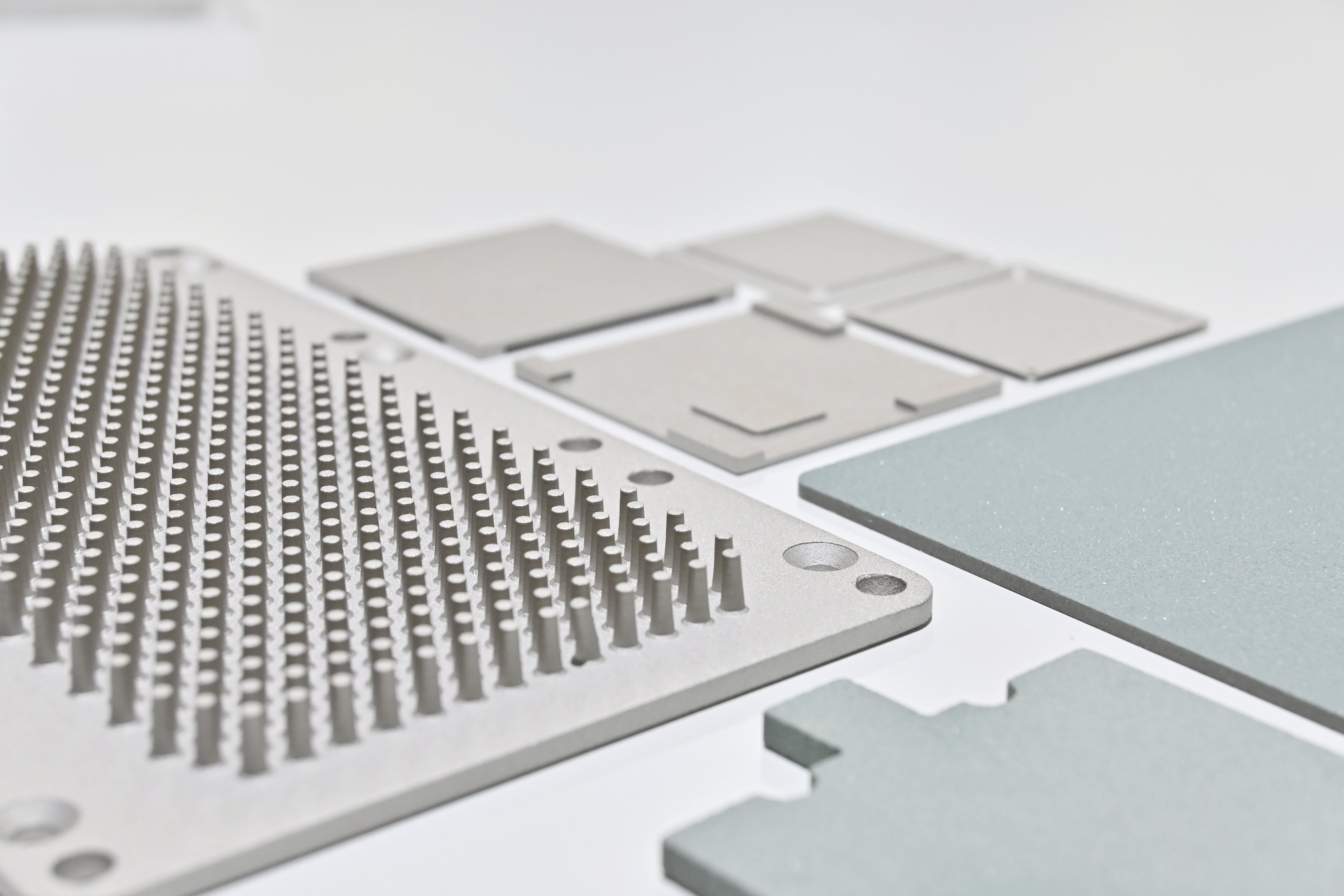
Copper spreads heat away from hotspots quickly, but conductivity alone does not determine package-level performance. Vapor chambers push effective spreading conductivity beyond solid metal by moving heat through evaporation and condensation, suiting packages where heat flux concentrates in a small footprint. Thickness, wick structure, and mechanical compatibility become the limiting factors.
Aluminum silicon carbide (AlSiC) balances spreading against dimensional stability. This ceramic matrix composite pairs relatively high thermal conductivity with a lower CTE than copper or aluminum, suiting applications where CTE compatibility and cycling reliability matter.
| Material | CTE (×10⁻⁶/K) |
|---|---|
| Silicon | ~2.6 |
| AlN substrate | 4.5 |
| Al₂O₃ substrate | 6.7 |
| AlSiC | 7-9 |
| Copper | 17.5 |
| Aluminum | 22.5 |
For mechanically sensitive packages, the best spreader is not the most conductive one. What matters more is the balance among thermal performance, CTE mismatch, warpage, interface stress, weight, and cycling reliability.
System-Level Cooling
Here the challenge shifts from moving heat through the package to rejecting it. Direct-to-chip liquid cooling and advanced cold plates offer greater capacity than air, but their effectiveness still depends on the thermal resistance of the interfaces and spreading structures between package and coolant.
Cold plate geometry is not a neutral variable either. A two-phase microchannel study of GPU and HBM co-cooling found that in a geometrically symmetric plate, the downstream GPU experienced heat transfer deterioration first because rising inlet vapor quality weakened liquid replenishment along the flow path. Symmetric hardware does not produce symmetric cooling once boiling begins. Since HBM stacks and logic dies sit at different heights, and different power densities on one substrate, channel layout and flow direction have to be co-designed with the package floorplan rather than fitted to it afterward.
Dynamic Thermal Control
Control strategies handle changing workloads and transient hotspots: sensors at critical locations, dynamic refresh-rate adjustment, firmware throttling past threshold, and per-channel power scaling. These augment rather than replace a well-engineered physical thermal path.
Why TIM Selection Decides the Outcome
TIM selection is one of the few variables still open in a large 2.5D module, and it carries considerable weight. Lid flatness variation, warpage, and uneven contact pressure degrade contact quality where it matters most, so the material must hold a repeatable bond line and absorb mechanical variation without pumping out over thousands of cycles. Each material class fits a specific position in the stack:
- Phase change materials pair low interface resistance with controlled bondline formation. Best for thin, large-area, mechanically sensitive stacks.
- High-conductivity gap fillers work across wider bond lines. Best where some assembly-height variability is acceptable.
- Curable gels offer conformability and reworkability on uneven surfaces and large tolerances, at the cost of higher interface resistance than phase change or metallic options.
- Graphite and graphene spreading layers move heat laterally away from concentrated hotspots, but are more sensitive to interface quality and flatness.
- Indium solder TIM reflows into an intermetallic bond for the lowest interfacial resistance available, with no pump-out. Requires backside metallization and an alloy chosen to survive downstream reflow.
- Gallium-based liquid metal conforms without clamping force and handles large height variation, but is electrically conductive, corrosive to aluminum and copper, and needs qualified barriers.
The right answer depends on gap tolerance, warpage behavior, assembly process, and rework requirements, so it is worth simulating before committing.
FAQs
What causes hotspots inside an HBM stack?
Three effects compound. The base logic die has the highest power density but sits at the bottom of the heat path, so its heat travels up through every DRAM die above it. Each inter-die gap is bridged by microbumps and underfill polymer, which conduct heat poorly, so resistance adds with stack height. The adjacent processor then heats the memory laterally through the interposer.
What temperature is too hot for HBM, and what happens past it?
DRAM-process dies are typically specified to 95°C junction temperature, below the 105°C commonly permitted for peripheral CMOS logic. Problems start well before that: retention time shortens as temperature rises, and above roughly 85°C parts commonly move to a doubled refresh rate. Past the safe limit, clocks and voltages are pulled back.
How much performance does an HBM hotspot actually cost?
More than the temperature reading suggests, because the loss compounds. Refresh cycles consume bandwidth that compute never sees. Higher utilization raises temperature further, shortening retention and forcing more refresh. The risk of unrecoverable memory errors also climbs, which matters most in long training runs.
Which thermal interface material works best for HBM packages?
It depends on the gap, warpage behavior, and assembly process, so the honest answer is to simulate before committing. In large 2.5D modules, phase change materials are a common starting point: low interface resistance, a controlled bond line, and tolerance for thin, large-area stacks. Where die heights differ, zoned or multi-layer schemes prevent one tall die from dictating a thick bond line everywhere else.
Can heat spreader material reduce CTE-related stress in an HBM package?
Yes, and it is an underused lever. Copper expands at 17.5×10⁻⁶/K against silicon at roughly 2.6×10⁻⁶/K, and that gap drives warpage, solder fatigue, and TIM pump-out. AlSiC sits at 7 to 9×10⁻⁶/K with thermal conductivity above 180 W/m·K, trading intrinsic conductivity for much lower interfacial stress. That trade is right when the limiting failure mode is mechanical rather than steady-state temperature.
Need Help With HBM Hotspot Management?
HBM hotspots are a systems problem: stack architecture, interface materials, spreading structures, and cooling all interact, and changing one shifts the others. T-Global USA works across the full path, from simulation and testing to custom thermal modules, TIMs, and AlSiC heat spreaders.
Contact us to talk through your package, or request a sample.
References
- Kothari, G., & Ghose, K. (2025). Addressing Thermal Throttling in HBM. In 2025 IEEE/ACM International Conference on Computer-Aided Design (ICCAD 2025) Conference Proceedings. Institute of Electrical and Electronics Engineers. https://doi.org/10.1109/ICCAD66269.2025.11240810
- JEDEC Solid State Technology Association. (April 2025). JEDEC and Industry Leaders Collaborate to Release JESD270-4 HBM4 Standard: Advancing Bandwidth, Efficiency, and Capacity for AI and HPC. https://www.jedec.org/news/pressreleases/jedec%C2%AE-and-industry-leaders-collaborate-release-jesd270-4-hbm4-standard-advancing
- SK hynix. (May 26, 2026). SK hynix Unveils ‘iHBM’ Thermal Solution to Boost AI Performance. SK hynix Newsroom. https://news.skhynix.com/en/ihbm-solution/
- Micron Technology, Inc. Semiconductor Die Assemblies With Enhanced Thermal Management, Semiconductor Devices Including Same and Related Methods. US Patent Application 20130119527. https://patents.justia.com/patent/20130119527
- PatSnap Insights. (2024). HBM4 Thermal Resistance Solutions in Stacked DRAM. https://www.patsnap.com/resources/blog/articles/hbm4-thermal-resistance-solutions-in-stacked-dram/
- Vinci. (August 2026). Full-Fidelity Thermal Simulation at Floorplanning Speed for 2.5D AI Accelerator Packages. Semiconductor Engineering. https://semiengineering.com/full-fidelity-thermal-simulation-at-floorplanning-speed-for-2-5d-ai-accelerator-packages/
- Tan, C. K., Ng, R. Y., Sethuraman, S., & Bains, K. S. *Per Channel Thermal Management Techniques for Stacked Memory.* US Patent 12,265,723 B2, granted April 1, 2025. Assignee: Intel Corporation. https://patents.google.com/patent/US12265723B2/en
- American Elements. Thermal Expansion Coefficient of Metals & Materials. https://www.americanelements.com/thermal-expansion-coe.html
- Kong, M. (July 2025). Engineering Reliable Heat Dissipation With Indium-Silver Thermal Interfaces. Amkor Technology / Semiconductor Engineering. https://semiengineering.com/engineering-reliable-heat-dissipation-with-indium-silver-thermal-interfaces/
- Long-Term Corrosion of Eutectic Gallium, Indium, and Tin (EGaInSn) Interfacing with Diamond. (2024). Materials, 17(11), 2683. https://www.mdpi.com/1996-1944/17/11/2683
- Ni, F., Zhang, S., Li, H., Zhang, Y., Ma, X., Yang, X., Wei, J., Qu, G., Liang, P., Zhu, Y., & Li, S. (2026). A two-phase microchannel cold plate system for AI data center GPUs: CHF-constrained GPU-HBM co-thermal management. https://papers.ssrn.com/sol3/papers.cfm?abstract_id=7089085