
Contents
- Heat Flux vs. Thermal Power vs. Thermal Resistance
- The Heat Flux Formula and Its Units
- Relating Heat Flux to TIM Thermal Impedance
- Average Heat Flux vs. Local Heat Flux and Hotspots
- Using Heat Flux as a Design-Review Trigger
- Applying Heat Flux to a Real Thermal Path
- FAQs
- References
Heat flux describes how concentrated thermal power is over a defined area. In electronics cooling, it is commonly expressed in W/cm² and governs interface temperature drop, thermal spreading, and hotspot severity.
Consider two devices that each dissipate 40 W. Spread across a 400 mm² surface, the average heat flux is 10 W/cm². If the same 40 W originates from a 4 mm² region, the average heat flux is 1,000 W/cm². The total thermal load is identical, but the local conduction and spreading requirements vary fundamentally.
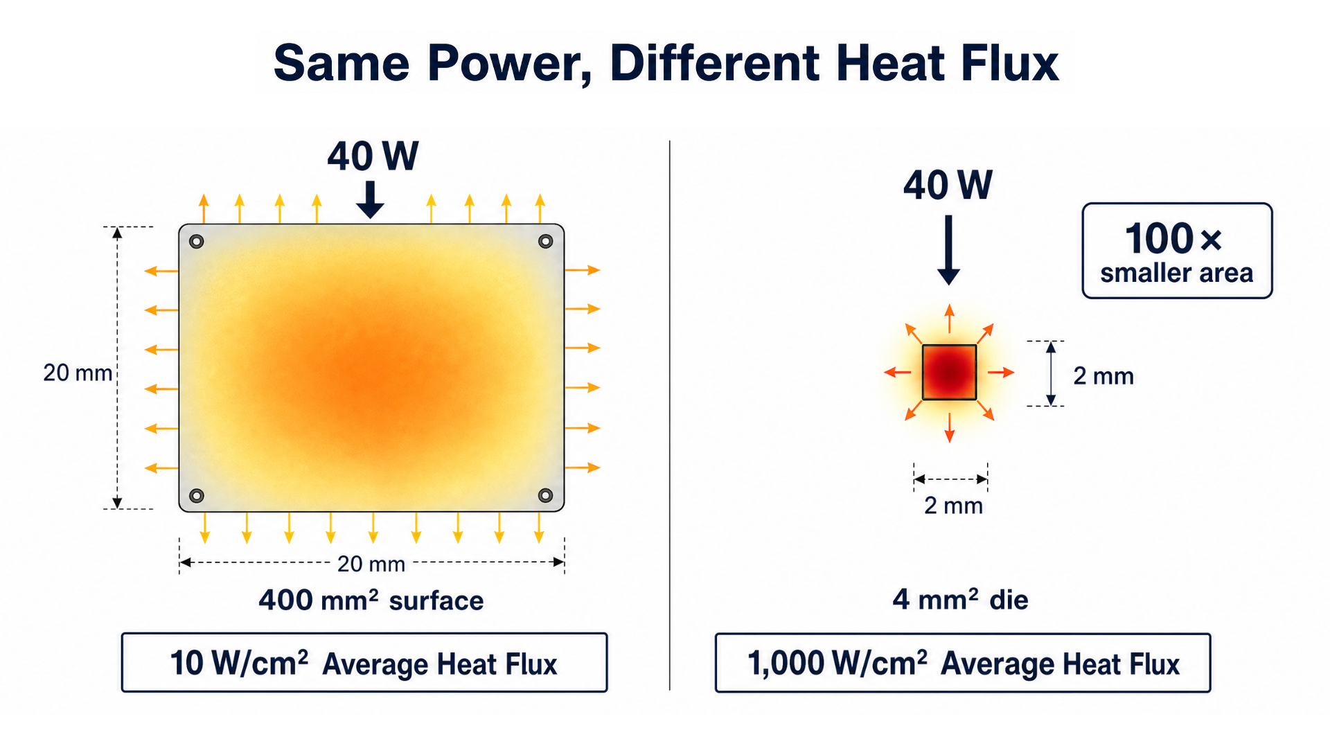
Total power tells you how much heat must ultimately be rejected. Heat flux tells you how concentrated that heat is at a particular point in the thermal path.
Heat Flux vs. Thermal Power vs. Thermal Resistance
Watts, heat flux, and thermal resistance get used in design discussions as though they were interchangeable. They answer different questions. Watts give the load size. Heat flux gives its concentration. Thermal resistance and impedance give the temperature rise that load produces along a path or across a layer. Most datasheets publish the first and leave the other two to the reader.
Table 1. Thermal quantities compared: what each one measures, its unit, and where it is used
| Quantity | What it tells the engineer | Typical unit | Primary use |
|---|---|---|---|
| Heat transfer rate, Q˙ | Rate at which heat must be removed | W | Overall cooler capacity, airflow, coolant load |
| Average heat flux, q̄″ | Heat transfer rate per unit area, averaged over a defined area | W/cm² | TIM loading, interface ΔT, thermal spreading |
| Local heat flux, q″(x,y) | Heat transfer rate per unit area at a point, normal to the surface | W/cm² | Hotspots, local temperature gradients, chip power maps, FEA/CFD |
| Thermal resistance, Rth | Temperature difference per unit heat transfer rate | °C/W | Component/system thermal path |
| Unit-area thermal resistance, R″th | Temperature difference per unit heat flux through the bulk of a layer, BLT/k, excluding contacts | °C·cm²/W | TIM bulk property |
| Thermal impedance, Z″th | Temperature difference across a layer per unit heat flux, including both contact resistances | °C·cm²/W | TIM evaluation |
The Heat Flux Formula and Its Units
Heat flux is the rate of thermal energy transfer per unit area. Strictly, heat flux is a point quantity that varies across a surface. Inside a solid, it follows Fourier’s law, q″ = −k∇T: the local temperature gradient ∇T is set by the flux and the material’s thermal conductivity k, not by total power. (Heat Conduction: Energy Transfer Through Solids, n.d.) Design work uses its average over a defined area:
Where q̄″ is the average heat flux (W/cm²), Q˙ is the heat transfer rate (W), and A is the cross-sectional area normal to the heat flow.
The SI unit is W/m². Electronics thermal work almost always uses W/cm², since the areas involved are small. Power electronics groups sometimes use W/mm² for die-level work.
Heat flux is not a single number for a given part
The formula is trivial. The ambiguity sits in the denominator, which is why two engineers can quote different flux figures for the same component and both be right.
Consider a 40 W device in a lidded package, with an 8 × 8 mm die inside a 35 × 35 mm lid.
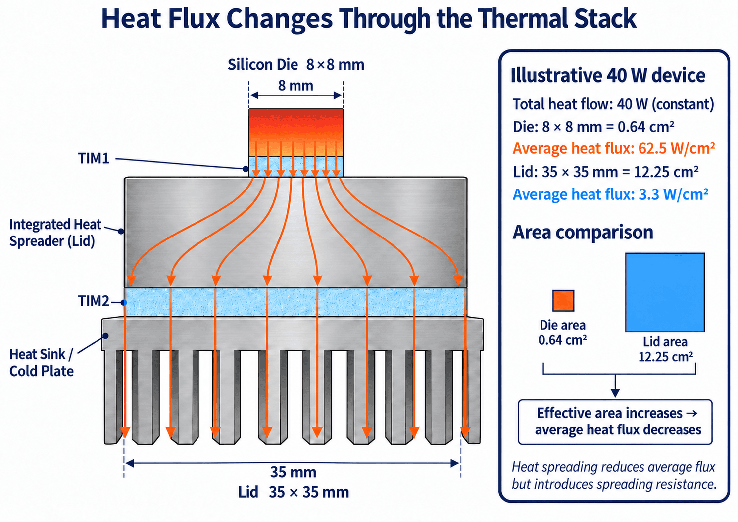
Table 2. Heat flux at two interfaces of the same 40 W package
|
Location in the Stack
|
Area
|
Average Heat Flux
|
|---|---|---|
|
Die surface (TIM1)
|
0.64 cm²
|
62.5 W/cm²
|
|
Lid surface (TIM2)
|
12.25 cm²
|
3.3 W/cm²
|
Same 40 W, a factor of 19 apart, across two interfaces separated by about two millimeters of copper. Neither number is wrong. They answer different questions.
The die-area figure is the highest flux in the stack and governs junction temperature. The lid footprint is what a TIM2 material sees, after the integrated heat spreader (IHS) has done most of the work. The heat sink base, or cold plate, gives a third number, usually an order of magnitude below the die, and it matters for sizing the rejection solution.
The numerator carries its own ambiguity. Thermal Design Power (TDP) is a design target, not a measurement, and heat splits between paths: a lidded flip-chip package sends most of its heat upward, while a bare-die BGA on heavy copper loses a meaningful fraction through the balls into the board. For power stages, the number that matters is the loss, not the throughput. Power delivered to the load does not heat the converter; only the inefficiency does. A 500 W converter at 96 percent efficiency turns about 4 percent of its input into heat, roughly 20 W, and that loss is split unevenly across switches, magnetics, and rectifiers. Each component has its own area, and therefore its own heat flux. A MOSFET dissipating a few watts on a small die can present a higher flux than a transformer dissipating several times more.
Heat flux changes at every step down the stack
The reduction in flux from die to lid is not free. It comes from thermal spreading, and spreading has a thermal cost.
When heat enters a plate through a small area and leaves through a larger one, the flow lines bend outward, adding a resistance term on top of the one-dimensional conduction through the plate thickness.
Two points follow from the spreading literature that matter in a design review:
- Spreading resistance grows as the source-to-sink area ratio gets more extreme.
- Both spreader thickness and conductivity help, with diminishing returns. Doubling the copper thickness does not halve the spreading resistance.
If die-level flux is high but your lid-level flux is comfortable, the package is spreading it for you, and your job is to protect that path with a low-impedance TIM. If your die-level flux is high and the package has no spreader, add one: a ceramic heat spreader, an AlSiC baseplate, a graphite sheet for in-plane transport, or a vapor chamber base. Adding fins to a heat sink starved by spreading resistance will not reduce junction temperature much.
Relating Heat Flux to TIM Thermal Impedance
ASTM D5470 characterizes thermal interface materials by thermal impedance, the temperature difference across a layer per unit heat flux, including the contact resistance at both surfaces. The standard specifies it in K·m²/W; datasheets usually quote °C·cm²/W, or °C·in²/W in the US, including ours (1 °C·in²/W = 6.45 °C·cm²/W, 1 W/cm² = 6.45 W/in²). (Standard Test Method for Thermal Transmission Properties of Thermally Conductive Electrical Insulation Materials, 2024) Notice what happens when you multiply that by heat flux:
Where heat flow through the interface is uniform and one-dimensional, the areas cancel, and multiplying heat flux by TIM thermal impedance gives the temperature drop across the interface directly. It takes one multiplication, with no resistance network to build. The cancellation only works if flux and impedance use the same area unit.
The impedance value must correspond to the relevant bond line thickness (BLT), assembly pressure, temperature, and test method. Real assemblies also introduce non-uniform flux, spreading resistance, and pressure variation.
Worked example: one material, four flux levels
Take a thin gap filler with a measured D5470 thermal impedance, Z″th, of 0.35 °C·cm²/W (0.054 °C·in²/W) at your assembly pressure and bond line thickness.
Table 3. Temperature drop across a single TIM (0.35 °C·cm²/W) at four heat flux levels
|
Heat Flux
|
ΔT across the TIM
|
|---|---|
|
5 W/cm²
|
1.8 °C
|
|
25 W/cm²
|
8.8 °C
|
|
60 W/cm²
|
21 °C
|
|
150 W/cm²
|
53 °C
|
The material did not change. At 5 W/cm², the TIM contributes a small rise under the stated conditions, and your attention belongs elsewhere. It is probably the largest single term in your budget when the heat flux reaches 60 W/cm². At 150 W/cm², it consumes your entire allowable rise before the heat sink can act. (Park et al., 2015)
Worked example: why bond line thickness dominates at high flux
Thermal impedance is the sum of a bulk term and the contact resistance at both surfaces: Z″th = BLT/k + R″contact. The bulk term, BLT/k, is the layer’s unit-area thermal resistance, R″th. A 1.0 mm pad at 3 W/m·K has an R″th of roughly 3.3 °C·cm²/W. The contact term, extrapolated to zero thickness under D5470, sits on top and can exceed the bulk term at thin bond lines. (Calculating Interface Resistance, 2023)
Table 4. Bulk temperature drop through a 1.0 mm, 3 W/m·K pad at two stack locations
|
Interface
|
Flux
|
Bulk ΔT (q̄″ × R″th) through a 1.0 mm, 3 W/m·K pad
|
|---|---|---|
|
Lid (TIM2)
|
3.3 W/cm²
|
~11 °C
|
|
Bare die (TIM1)
|
62.5 W/cm²
|
~208 °C
|
That second number is not a real design. It shows why a 1 mm gap pad is unsuitable for a direct bare-die interface at this flux. Once flux climbs, you compress the bond line and switch material class: from a thick gap pad to thermal grease, a phase change material, or a dispensed curable thermal gel that can hold a bond line under 100 µm.
Average Heat Flux vs. Local Heat Flux and Hotspots
Average heat flux can hide two effects: spatial concentration and temporal concentration.
Spatial concentration occurs when heat generation is non-uniform across a die or package. Localized hotspots reach substantially higher heat flux than the die average, while averaging across a multi-die module can further mask these peaks.
Temporal concentration occurs when pulsed or intermittent loads produce short-duration peak heat flux above the time-averaged value. Whether the peak or average condition governs depends on pulse duration, duty cycle, and the thermal mass along the path, which is why pulsed loads are modeled with an RC network and a transient Zth(t) curve rather than a single resistance.
The same caution applies to the package metrics printed on a datasheet, though the word impedance shifts meaning along the way. ASTM D5470 uses it for the steady-state, area-normalized Z″th used earlier; JEDEC uses it for the transient Zth(t) curve just described. JEDEC thermal resistance values are defined for standardized boards and environments, which makes them comparable across parts but prevents them from describing either form of concentration. θJA suits package comparison and should not be read as a prediction of junction temperature in an actual system. (Guenin, 2013) JESD51-12.01 guides interpreting package thermal information, while JESD51-14 extracts θJC from a transient dual-interface measurement for devices with a dominant case-side heat-flow path, a narrower and more transferable claim than θJA makes. (Bornoff, 2024; Theta-JC Measurements, 2024)
Using Heat Flux as a Design-Review Trigger
The following bands are not hard limits. Published reviews of high-flux cooling report wide overlaps between technologies depending on allowable temperature rise, coolant, and geometry. Treat them as prompts, not a selection chart.
Table 5. Heat flux bands and the design questions each one raises
|
Approximate Flux at the Interface
|
What Usually Deserves A Second Look
|
|---|---|
|
Below 1 W/cm²
|
Natural convection is often sufficient. TIM choice is driven by assembly, gap tolerance, and cost, not thermal performance. |
|
1 to 10 W/cm²
|
Standard extruded or bonded-fin heat sink with a conventional gap pad. TIM impedance is a minor term. |
|
10 to 50 W/cm²
|
Spreading resistance and TIM impedance both become material. Compress the bond line, verify D5470 data at your actual pressure, and check whether the spreader is the bottleneck. |
|
50 to 150 W/cm²
|
Two-phase spreading (vapor chamber or embedded heat pipes) frequently earns its cost. TIM selection moves toward greases, PCMs, and gels with impedance under 0.2 °C·cm²/W. |
|
Above 150 W/cm²
|
Liquid cold plates, direct liquid attach, or specialized approaches. Interface impedance becomes a first-order design variable, and metal TIMs enter consideration. |
The boundaries themselves are arguable. The dependency is not: the table is unusable without a flux figure, and there is no flux figure until you decide which area you are dividing by.
Applying Heat Flux to a Real Thermal Path
T-Global USA supports thermal interface selection, heat spreading, material customization, and application-level thermal evaluation.
Flux determines which material class is worth evaluating, which usually means one of four conversations:
- Moderate flux with mechanical tolerance to absorb. Thermal pads and thermal putty handle variable gaps without loading the board.
- High flux with a thin, controlled bond line. Thermal grease, phase change materials, and curable thermal gels minimize the impedance term where it matters most.
- High-flux applications that need spreading before rejection. Graphite, graphene, ceramic spreaders, and AlSiC reduce flux before it reaches the interface.
- Very high flux, where even a polymer layer costs too much temperature. Metal TIMs reach lower interface impedance than polymer materials, but bring reliability and material-compatibility constraints. T-Global USA is preparing indium foil and liquid metal TIM solutions; see when a metal TIM pays off.
You can also request samples to validate against your own test fixture.
FAQs
How do I calculate heat flux for an electronic component?
Divide the dissipated power by the interface area you are analyzing. A 25 W device on a 10 × 10 mm die gives 25 W ÷ 1 cm² = 25 W/cm². Area matters as much as power, since flux at the die differs from flux at the lid or the heat sink base.
Which area should I use, the die or the package?
Whichever interface you are asking about. Die area governs junction temperature and TIM1 selection, lid footprint governs TIM2 and heat sink selection, and heat sink base area sizes the rejection solution. Flux drops at each step because the package spreads the heat.
What counts as high heat flux?
There is no universal threshold. Most air-cooled commercial electronics sit below 10 W/cm² at the heat sink interface. Above roughly 50 W/cm², spreading and interface impedance become first-order variables, and two-phase or liquid approaches enter the conversation. (Qu & Mudawar, 2003, pp. 598-609) What matters is your allowable temperature rise, not the flux alone.
How does heat flux relate to TIM thermal impedance?
Directly. TIM impedance from ASTM D5470 is usually quoted in °C·cm²/W or °C·in²/W. Multiply by heat flux in the same area unit, and the areas cancel, leaving the temperature drop across the interface in °C. That is the TIM’s contribution to your thermal budget, in one calculation.
Does a higher W/m·K thermal pad always reduce temperature?
No. Impedance depends on thickness and conductivity, plus contact resistance at both surfaces. A 1.0 mm pad at 6 W/m·K has a higher bulk term, BLT/k, than a 0.25 mm pad at 3 W/m·K: 1.7 versus 0.8 °C·cm²/W. At low flux, the difference is often irrelevant; at high flux, it decides the design. Compare impedance at your pressure and thickness, not conductivity alone.
References
- (n.d.). Heat Conduction: Energy Transfer Through Solids. Quadco Engineering. https://www.quadco.engineering/en/know-how/heat-transfer-conduction.htm
- Bornoff, R. (April 2, 2024). The Applicability of JESD51-14 for the Determination of Junction-to-Case Thermal Resistance. Electronics Cooling. https://www.electronics-cooling.com/2024/04/the-applicability-of-jesd51-14-for-the-determination-of-junction-to-case-thermal-resistance/
- (2024). Standard Test Method for Thermal Transmission Properties of Thermally Conductive Electrical Insulation Materials. ASTM D5470-17(2024). https://doi.org/10.1520/D5470-17
- (2023). Calculating Interface Resistance. Electronics Cooling. https://www.electronics-cooling.com/2023/02/calculating-interface-resistance-2/
- Guenin, B. (2013). Use of JEDEC Thermal Metrics in Calculating Chip Temperatures (without Attached Heat Sinks). Electronics Cooling. https://www.electronics-cooling.com/2013/12/use-jedec-thermal-metrics-calculating-chip-temperatures-without-attached-heat-sinks/
- Park, W., Guo, Y., Li, X., Hu, J., Liu, L., Ruan, X. & Chen, Y. P. (2015). High-performance Thermal Interface Material Based on Few-layer Graphene Composite. arXiv preprint arXiv:1511.00076. https://doi.org/10.48550/arXiv.1511.00076
- Qu, W. & Mudawar, I. (2003). Thermal Design Methodology for High-Heat-Flux Single-Phase and Two-Phase Micro-Channel Heat Sinks. IEEE Transactions on Components and Packaging Technologies, 26(3), 598–609. / (Qu & Mudawar, 2003) https://doi.org/10.1109/TCAPT.2003.817652
- Theta-JC measurements: Steady-state compared to transient methods. (2024). Electronics Cooling. https://www.electronics-cooling.com/2024/11/theta-jc-measurements-steady-state-compared-to-transient-methods/